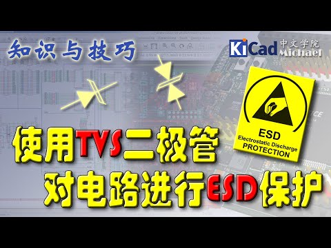
參考內容推薦

[PDF] Optimized Layout on ESD Protection Diode with Low Parasitic ...

In this work, the ESD protection diodes realized in waffle, multi-waffle, and multi-waffle-hollow layout styles are fabricated in a 90-nm CMOS process.

[PDF] PCB Layout for TVS Diodes

Place the TVS diode close to the ESD entry source. 3. Connect the TVS diode to the ground of the power supply or chassis. 1. Minimize the parasitic ...

Layout guidelines for optimized ESD protection diodes

In this work, various layout options for ESD diodes' PN junction geometry and metal routing are investigated. The current compression point (ICP) is ...

Beginner's Guide to ESD Protection Circuit Design for PCBs

Here are some ESD protection circuit design options you can use in your next PCB and some PCB layout best practices for your new product.

Where to Place TVS Diodes in a PCB Layout

In this article, we'll show where to place a TVS diode in a PCB layout, particularly near connectors mounted along a board edge.

5 Layout considerations for TVS diodes (ESD protection diodes)

1. Place ESD protection diodes close to the ESD entry point. 2. Minimize trace inductance in series with ESD protection diodes including GND.

[PDF] PCB Design Guidelines that Maximize the Performance of TVS Diodes

Designing in EMI and ESD protection at the beginning of the project saves time and money, as shown in Figure 1. This is a simple concept, but often surge ...

[PDF] AN5686

The best way to minimize these issues is to place transient voltage suppressors (TVS) from ST, where the surges can appear; but some care must ...

[PDF] ESD Protection Layout Guide (Rev. A)

ESD selection guides are available in Technical Documents at www.ti.com/esd for guidance in choosing the correct type of TVS diode for a particular system.

[PDF] ESD Packaging and Layout Guide (Rev. B)

By splitting into three sections, this guide helps with selecting the proper transient voltage suppressor (TVS) for ESD protection in a system design. The first ...

esddiodelayout

Inthiswork,theESDprotectiondiodesrealizedinwaffle,multi-waffle,andmulti-waffle-hollowlayoutstylesarefabricatedina90-nmCMOSprocess.,PlacetheTVSdiodeclosetotheESDentrysource.3.ConnecttheTVSdiodetothegroundofthepowersupplyorchassis.1.Minimizetheparasitic ...,Inthiswork,variouslayoutoptionsforESDdiodes'PNjunctiongeometryandmetalroutingareinvestigated.Thecurrentcompressionpoint(ICP)is ...,Hereareso...